- 您现在的位置:买卖IC网 > Sheet目录337 > LE25U20AMB-AH (ON Semiconductor)IC MEM 2MBIT SERIAL FLASH 8SOP
�� �
�
�LE25U20AMB�
�Description� of� Commands� and� Their� Operations�
�"Table� 2� Command� Settings"� provides� a� list� and� overview� of� the� commands.� A� detailed� description� of� the� functions� and�
�operations� corresponding� to� each� command� is� presented� below.�
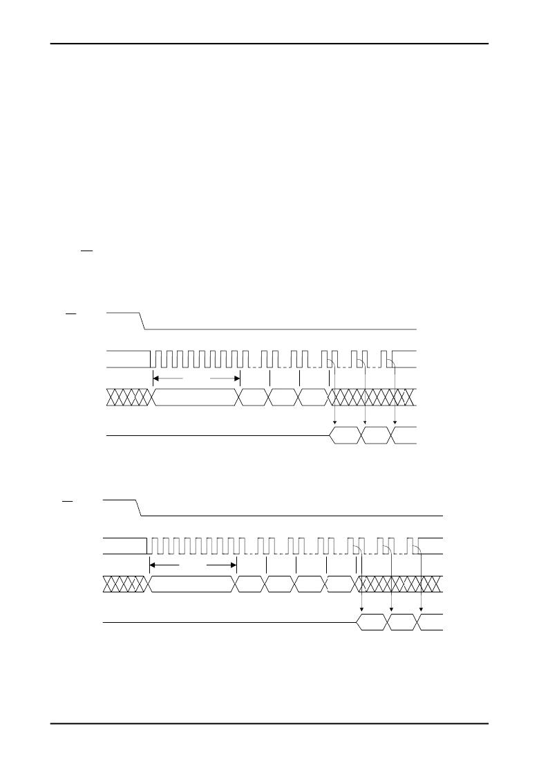
�1.� Read�
�There� are� two� read� commands,� the� 4� bus� cycle� read� command� and� 5� bus� cycle� read� command.� Consisting� of� the� first�
�through� fourth� bus� cycles,� the� 4� bus� cycle� read� command� inputs� the� 24-bit� addresses� following� (03h),� and� the� data� in� the�
�designated� addresses� is� output� synchronized� to� SCK.� The� data� is� output� from� SO� on� the� falling� clock� edge� of� fourth� bus�
�cycle� bit� 0� as� a� reference.� "Figure� 5-a� 4� Bus� Read"� shows� the� timing� waveforms.�
�Consisting� of� the� first� through� fifth� bus� cycles,� the� 5� bus� cycle� read� command� inputs� the� 24-bit� addresses� and� 8� dummy�
�bits� following� (0Bh).� The� data� is� output� from� SO� using� the� falling� clock� edge� of� fifth� bus� cycle� bit� 0� as� a� reference.�
�"Figure� 5-b� 5� Bus� Read"� shows� the� timing� waveforms.� The� only� difference� between� these� two� commands� is� whether� the�
�dummy� bits� in� the� fifth� bus� cycle� are� input.�
�When� SCK� is� input� continuously� after� the� read� command� has� been� input� and� the� data� in� the� designated� addresses� has�
�been� output,� the� address� is� automatically� incremented� inside� the� device� while� SCK� is� being� input,� and� the� corresponding�
�data� is� output� in� sequence.� If� the� SCK� input� is� continued� after� the� internal� address� arrives� at� the� highest� address�
�(3FFFFh),� the� internal� address� returns� to� the� lowest� address� (00000h),� and� data� output� is� continued.� By� setting� the� logic�
�level� of� CS� to� high,� the� device� is� deselected,� and� the� read� cycle� ends.� While� the� device� is� deselected,� the� output� pin� SO�
�is� in� a� high-impedance� state.�
�Figure� 5-a� 4� Bus� Read�
�CS�
�Mode3�
�0� 1� 2� 3� 4� 5� 6� 7� 8�
�15� 16�
�23� 24�
�31� 32�
�39� 40�
�47�
�SCK�
�Mode0�
�8CLK�
�SI�
�03h�
�Add.�
�Add.�
�Add.�
�N�
�N+1�
�N+2�
�SO�
�High� Impedance�
�DATA�
�MSB�
�DATA�
�MSB�
�DATA�
�MSB�
�Figure� 5-b� 5� Bus� Read�
�CS�
�Mode3�
�0� 1� 2� 3� 4� 5� 6� 7� 8�
�15� 16�
�23� 24�
�31� 32�
�39� 40�
�47� 48�
�55�
�SCK�
�Mode0�
�8CLK�
�SI�
�0Bh�
�Add.�
�Add.�
�Add.�
�X�
�N�
�N+1�
�N+2�
�SO�
�High� Impedance�
�DATA�
�MSB�
�DATA�
�MSB�
�DATA�
�MSB�
�No.A2097-6/21�
�发布紧急采购,3分钟左右您将得到回复。
相关PDF资料
LFDAS12XSIT
HARDWARE MC9S12XS 112-PIN
LFXP10E-L-EV
BOARD EVAL LATTICEXP10E STD
LH28F008SCHT-TE
IC FLASH 8MBIT 85NS 40TSOP
LH28F160S3HNS-TV
IC FLASH 16MBIT 100NS 56SSOP
LH28F160S5HNS-S1
IC FLASH 16MBIT 70NS 56SSOP
LH28F320S3HNS-ZM
IC FLASH 32MBIT 110NS 56SSOP
LH28F320SKTD-ZR
IC FLASH 32MBIT 70NS 48TSOP
LHF00L28
IC FLASH 16MBIT 70NS 48TSOP
相关代理商/技术参数
LE25U20AMBM02-AH
功能描述:闪存 RoHS:否 制造商:ON Semiconductor 数据总线宽度:1 bit 存储类型:Flash 存储容量:2 MB 结构:256 K x 8 定时类型: 接口类型:SPI 访问时间: 电源电压-最大:3.6 V 电源电压-最小:2.3 V 最大工作电流:15 mA 工作温度:- 40 C to + 85 C 安装风格:SMD/SMT 封装 / 箱体: 封装:Reel
LE25U40CFQ-AH
制造商:ON Semiconductor 功能描述:REEL / S-FLASH MEMORY(4M)
LE25U40CMC
制造商:SANYO 制造商全称:Sanyo Semicon Device 功能描述:4M-bit (512K??8) Serial Flash Memory
LE25U40CMC-AH
功能描述:闪存 S-FLASH MEMORY(4M)
RoHS:否 制造商:ON Semiconductor 数据总线宽度:1 bit 存储类型:Flash 存储容量:2 MB 结构:256 K x 8 定时类型: 接口类型:SPI 访问时间: 电源电压-最大:3.6 V 电源电压-最小:2.3 V 最大工作电流:15 mA 工作温度:- 40 C to + 85 C 安装风格:SMD/SMT 封装 / 箱体: 封装:Reel
LE25U40CMCQ00-AH
制造商:ON Semiconductor 功能描述:Flash S-FLASH MEMORY(4M)
LE25U40CQE
制造商:SANYO 制造商全称:Sanyo Semicon Device 功能描述:4M-bit (512K??′8) Serial Flash Memory
LE25U40CQE-AH
功能描述:电可擦除可编程只读存储器 RoHS:否 制造商:Atmel 存储容量:2 Kbit 组织:256 B x 8 数据保留:100 yr 最大时钟频率:1000 KHz 最大工作电流:6 uA 工作电源电压:1.7 V to 5.5 V 最大工作温度:+ 85 C 安装风格:SMD/SMT 封装 / 箱体:SOIC-8
LE25U40CQES00-AH
制造商:ON Semiconductor 功能描述:S-FLASH MEMORY(4M)